The working principle of the Silicon Drift Detector (SDD) is based on the concept of sideward depletion invented by Pavel Rehak and Emilio Gatti in 1983. It allows the depletion of a large volume of high-resistivity silicon material by a small anode receiving a minimum signal capacitance. By that, the SDD overcomes the major problem of a classical p-i-n diode detector where the input capacitance is direct proportional to the active area. Below figure? shows a schematic view of the SDD in its standard configuration :
硅漂移探測器(SDD)的工作原理基于Pavel Rehak和Emilio Gatti于1983年發明的側向耗盡概念。它允許通過接收最小信號電容的小陽極來耗盡大體積的高電阻率硅材料。通過這一點,SDD克服了經典p-i-n二極管檢測器的主要問題,其中輸入電容與有源面積成正比。下圖顯示了標準配置下SDD的示意圖。
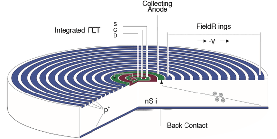
While the back contact is made up by a homogeneous, shallow p+n junction on the side where the incoming radiation enters the detector, the opposite side is characterized by a structure of circular p+ drift rings and eventually an integrated first FET for on-chip amplification. By applying a negative voltage on the radiation entrance window and an increasingly negative voltage on the drift rings, a potential field distribution is created such that the electrons generated by the ionizing radiation drift towards the small sized collecting anode situated in the center of the device. In the case of an integrated FET, the signal is directly amplified without adding any additional noise or microphony problems by bond wires.
雖然背接觸由入射輻射進入探測器一側的均勻淺p+n結組成,但相反一側的特征是圓形p+漂移環的結構,以及最終用于片上放大的集成第一FET。通過在輻射入射窗上施加負電壓并在漂移環上施加越來越負的電壓,產生了電勢場分布,使得由電離輻射產生的電子向位于器件中心的小尺寸收集陽極漂移。在集成FET的情況下,信號被直接放大,而不添加任何額外的噪聲或鍵合線的微光學問題。
Key Features
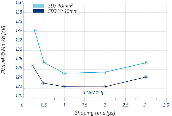
Best energy resolution?down to 121 eV @ Mn-Kα, – 30°C
Polysilicon technology?for ultra-low leakage current values < 100 pA/cm2, enabling high performance spectroscopy close to room temperature
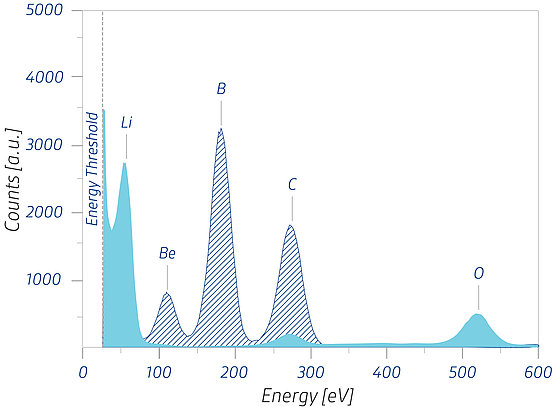
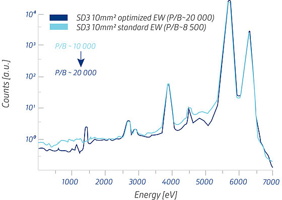
pnWindow?for the best light element detection and optimum P/B ratio up to 20 000
Wide selection of chip sizes and detector housings?5, 10, 20, 30, 60, 80, 100, 200, 300, 600 mm2
Unique shapes?like our Rococo Series and the Rococo Detectors
High count rates?up to 1 Mcps with single cells and several Mcps with our monolithic Multi-Element SDDs
Radiation hardness?>1014?Photons/cm2
主要功能
最佳能量分辨率低至121 eV@Mn-Kα,-30°C
超低漏電流值<100 pA/cm2的多晶硅技術,實現接近室溫的高性能光譜
pnWindow可實現最佳的光元件檢測和高達20000的最佳P/B比
廣泛選擇芯片尺寸和探測器外殼5、10、20、30、60、80、100、200、300、600 mm2
獨特的形狀,如我們的Rococo系列和Rococo探測器
單探測器高計數率高達1 Mcps,單片多元件SDD高計數率達數Mcps
輻射硬度>1014光子/cm2